JLARC Final Report: 2016 Tax Preference Performance Reviews
Report 17-02, January 2017
Semiconductor Materials Manufacturing | Multiple Taxes
- Summary of this Review
- Details on this Preference
- Recommendations and Agency Response
- How We Do Reviews
- More about this Review
| The Preference Provides | Tax Type | Estimated Biennial Beneficiary Savings |
|---|---|---|
| For the two preferences in use: | ||
| A reduced business and occupation (B&O) rate for manufacturing semiconductor materials. Beneficiaries pay a rate of 0.275 percent, compared to the general manufacturing rate of 0.484 percent. This preference is scheduled to expire December 1, 2018. | B&O Tax RCW 82.04.2404 |
Not Disclosable |
| A sales and use tax exemption for purchases of gases and chemicals used in specific phases of the semiconductor production process. This preference is scheduled to expire December 1, 2018. |
Sales and Use Tax RCW 82.08.9651, 82.12.9651 |
$3.2 million |
|
For the six Preferences not yet in effect: (Expiration dates contingent on date exemptions are utilized) |
||
| A sales and use tax exemption for the construction of new buildings used for manufacturing semiconductor materials. | Sales and Use Tax RCW 82.08.965, 82.12.965 |
$0 |
| A property tax exemption for machinery and equipment used for manufacturing semiconductor materials when located in a building exempted from sales tax. | Property Tax RCW 84.36.645 |
$0 |
| A B&O tax credit of $3,000 for each manufacturing production job located in a building exempted from sales tax. | B&O Tax RCW 82.04.448 |
$0 |
| A reduced B&O tax rate for manufacturing semiconductor materials. Beneficiaries would pay a rate of 0.275 percent compared to the general manufacturing rate of 0.484 percent for twelve years after its effective date. | B&O Tax RCW 82.04.240(2) |
$0 |
| A sales and use tax exemption for purchases of gases and chemicals used in the production of semiconductor materials for twelve years after its effective date. | Sales and Use Tax RCW 82.08.970, 82.12.970 |
$0 |
| A full B&O tax exemption for manufacturing semiconductor microchips. | B&O Tax RCW 82.04.426 |
$0 |
| Public Policy Objective |
|---|
| The Legislature stated its intent for this preference was to induce significant construction projects, retain, expand and attract semiconductor businesses, and create family wage jobs. |
| Recommendations |
|---|
|
For the two preferences in use:
Review and Clarify: While there has been one significant construction project, it is unclear what employment outcomes the Legislature wants to achieve. As part of the clarification, the Legislature should add uniform reporting requirements and targets for employment growth and wages to facilitate future reviews. |
|
For the six preferences not yet in effect:
Terminate: They have not been used in the thirteen years since they were enacted. Commissioner Recommendation: The Commission endorses the Legislative Auditor’s recommendation. In addition to JLARC staff’s research, a recent research paper released by the Congressional Research Service (CRS) on the U.S. semiconductor industry highlights some important points. First, the CRS study finds that about 87% of fabrication is located outside of the U.S. with little evidence this will change significantly in the future. Second, between 2001 and 2015 U.S. employment in semiconductor manufacturing has fallen 38%. Third, the decline in employment reflects both the shift of production to outside of the U.S.; increasing automation of production facilities; and a shift in favor of U.S. employment focused on semiconductor design work. The trends laid out by the CRS paper suggest that the current set of preferences will be, for the foreseeable future, underutilized or not utilized. |
- What is the Preference?
- Legal History
- Other Relevant Background
- Public Policy Objectives
- Are Objectives Being Met?
- Beneficiaries
- Reporting Issues
- Revenue and Economic Impacts
- Other States with Similar Preference?
- Applicable Statutes
This review covers eight tax preferences related to the semiconductor materials manufacturing industry. A semiconductor is a substance like silicon with electrical properties that make it ideal for use in electronic circuits. The term also applies to the devices made of these substances.
The Legislature’s intent is that the preferences induce significant construction projects; retain, expand, and attract semiconductor businesses; and encourage and expand family wage jobs.
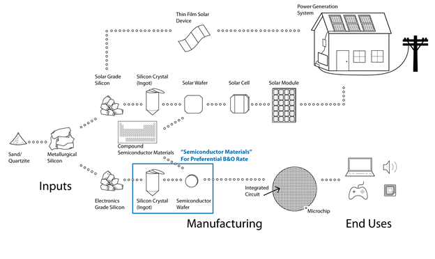
The Legislature chose different definitions of “semiconductor materials” for different preferences. As a result, the preferences vary in where they apply in the manufacturing process. The descriptions and exhibits below identify the different definitions and illustrate the steps in the manufacturing process that are covered by the different preferences.
Two of the eight preferences are currently in use. Six of the preferences are not currently in use because there has not been a required level of investment from a semiconductor business to trigger their taking effect.
Two Preferences in Use
Manufacturers of semiconductor materials and businesses that perform manufacturing services on semiconductor materials owned by others (known as “processors for hire”) receive the following:
- A reduced business and occupation (B&O) rate for manufacturing semiconductor materials. Beneficiaries pay a rate of 0.275 percent, compared to the general manufacturing rate of 0.484 percent. They are required to file an Annual Report with the Department of Revenue (DOR).
- A sales and use tax exemption for purchases of gases and chemicals used in specific phases of the semiconductor production process, such as:
- Growing or cleaning semiconductor materials, and other procedures where the gases and chemicals come into direct contact with the materials, or
- Cleaning the chambers and other equipment in which processing takes place.
Beneficiaries are required to report their tax savings and some employment information on an Annual Survey with DOR, unless they are already required to file an Annual Report for use of the B&O preference. Annual Reports include employment information. Beneficiaries who do not file an Annual Survey must file a Buyer Addendum, which states the value of the exempt items purchased.
Both of these preferences expire on December 1, 2018.
Reduced B&O Rate
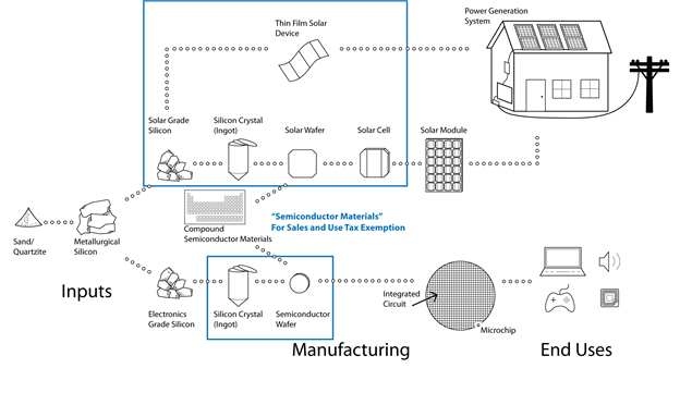
For the reduced B&O rate, the Legislature defined semiconductor materials to mean silicon crystals, silicon ingots, raw polished semiconductor wafers, and compound semiconductor wafers. The exhibit below shows the supply chain and manufacturing process for semiconductors from inputs through end uses. The box highlights the steps in the process where a semiconductor manufacturer or processor for hire can benefit from the B&O tax preference. See the Other Relevant Background tab for a more detailed explanation of this graphic.
Sales & Use Tax Exemption
For the sales and use tax exemption, the Legislature included the same definition of semiconductor materials as used for the reduced B&O rate but later expanded the definition to include materials that are used in solar energy systems. These include solar grade silicon, silicon solar wafers, compound semiconductor solar wafers, silicon solar cells, and thin film solar devices. The expansion of this preference expires on June 30, 2017.
The exhibit below shows the same supply chain and manufacturing process as shown earlier, with the boxes highlighting the larger area where a semiconductor manufacturer or processor for hire can benefit from the sales and use tax exemption.
Six preferences are not in effect:
The following six tax preferences were enacted in 2003 but will not go into effect until a firm makes an investment of at least $1 billion in new buildings, machinery and equipment to site and operate a semiconductor microchip fabrication facility. The investment has not yet occurred.
The first three preferences would reduce the tax obligations of semiconductor businesses locating or expanding in Washington:
- A sales and use tax exemption for the construction of new buildings used for manufacturing semiconductor materials. The preference applies to materials that become part of the building, and labor and services to install that property. The preference requires an employer to maintain at least 75 percent of full employment for eight years. Beneficiaries must pay back one eighth of the preference for each year in which the employment target is not met.
- A property tax exemption for machinery and equipment used for manufacturing semiconductor materials when located in a building exempted from sales tax.
- A B&O tax credit of $3,000 for each manufacturing production job located in a building exempted from sales tax. The credit applies for each year the job is maintained up to a maximum of eight years.
The remaining three preferences would reduce the tax obligations of businesses based on their daily operations, without regard to whether they built a new building.
- A reduced B&O tax rate for manufacturing semiconductor materials. Beneficiaries would pay a rate of 0.275 percent compared to the general manufacturing rate of 0.484 percent for twelve years after its effective date.
- A sales and use tax exemption for purchases of gases and chemicals used in the production of semiconductor materials for twelve years after its effective date.
- A full B&O tax exemption for manufacturing semiconductor microchips. This preference would only apply to the steps in the manufacturing process that result in the production of a microchip. This preference would apply for nine years after its effective date.
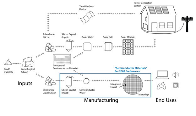
These preferences define semiconductor materials as silicon crystals, silicon ingots, raw polished semiconductor wafers, and compound semiconductor wafers, integrated circuits and microchips. The full B&O exemption only applies to the manufacturing of semiconductor microchips.
The exhibit below shows the same supply chain and manufacturing process for semiconductors as was used to describe the two preferences that are in use, with the boxes highlighting the different definition of semiconductor materials.
All six of the preferences enacted in 2003 would require beneficiaries to file an Annual Report to DOR detailing their employment information if they were in effect.
2001
Governor Locke’s Washington Competitiveness Council identified the semiconductor industry as an important industry cluster for the state’s economy. A common definition of an industry cluster is a geographic concentration of interconnected companies in a particular field. It may include suppliers, producers, providers, and other related entities.
2003
The Legislature enacted a package of six preferences targeting the semiconductor cluster. These preferences only become effective if a firm makes an investment of at least $1 billion in new buildings, machinery and equipment to site and operate a semiconductor microchip fabrication facility.
When enacting these preferences, the Legislature indicated that additional incentives were needed in light of the unique forces and global issues involved in the cluster, and that businesses in Washington were facing pressure to expand elsewhere.
During legislative hearings for these preferences, representatives from one semiconductor manufacturer (Wafertech) testified that the business was considering investing $3.5 billion in a new facility to produce 12 inch wafers. They indicated that the technology in their existing 8 inch wafer facility would be obsolete in 8 to10 years and that their parent company would have to make a decision on whether or not to remain at the site if that happened.
The bill’s prime sponsor stated:
…one particular employer in Southwest Washington, whom without this we probably don’t stand a strong chance of keeping that employer down the road, currently employs about 900 individuals and that number is going to go up to 1,200 with an average salary of around $60,000 a year with full benefits…that’s $54 million a year just in payroll going into the local economy that you stand to lose, not to mention the growth and other jobs that grow around these types of centers.
In the intent statement for the bill, the Legislature cited the Washington Competitiveness Council’s identification of semiconductors as a key industry cluster.
The required level of investment did not take place, and the preferences did not take effect.
2006
The Legislature enacted two new semiconductor preferences. These preferences were nearly identical in language to the 2003 preferential B&O tax rate and the sales and use tax exemption for gases and chemicals, with two notable differences:
- In the new (2006) preferences, the Legislature excluded microchips and integrated circuits from the definition of semiconductor materials. These materials were specifically targeted in the 2003 preferences;
- The preferences were contingent on different amounts of capital investment. The 2003 preferences required at least one business to make a minimum investment of $1 billion in a semiconductor microchip fabrication facility, while the 2006 preferences required an investment of $350 million by a semiconductor materials fabrication facility in order for the preferences to take effect.
Legislative testimony and newspaper reports at the time the preferences passed indicate that one semiconductor firm in particular, S E H America, was considering a large investment in Washington.
Unlike the 2003 preferences, a semiconductor business did make the required minimum investment to put the 2006 preferences into effect. The Department of Revenue gave notice that the preferences were in effect as of December 1, 2006.
Both the reduced B&O rate and the sales and use tax exemption include an expiration date of December 1, 2018.
2009
The Legislature expanded the definition of semiconductor materials for the 2006 sales and use tax exemption. The new definition included solar wafers, silicon solar cells and thin film solar devices. The provision was part of a larger bill expanding solar tax preferences.
2013
The Legislature further expanded the definition of semiconductor materials for the sales and use tax exemption to include the manufacturing of solar grade silicon. In the same bill, the Legislature extended a different preference for solar silicon manufacturers. That preference, and the expansion of semiconductor materials, are both are scheduled to expire in 2017. JLARC staff are reviewing the preference for solar silicon manufacturing in 2016.
This same legislation amended reporting requirements for beneficiaries of the preferential B&O rate. The beneficiaries were required to file an Annual Survey with DOR, reporting their tax savings and some employment information. Beneficiaries of the sales and use tax exemption were still required to file an Annual Report with employment information, and any taxpayer claiming both preferences was required to file both.
2014
The Legislature changed the reporting requirements to allow manufacturers claiming both the B&O tax preferential rate and the sales and use tax exemption to file only the Annual Report with DOR. Beneficiaries not filing an Annual Survey are required to file a Buyer Addendum.
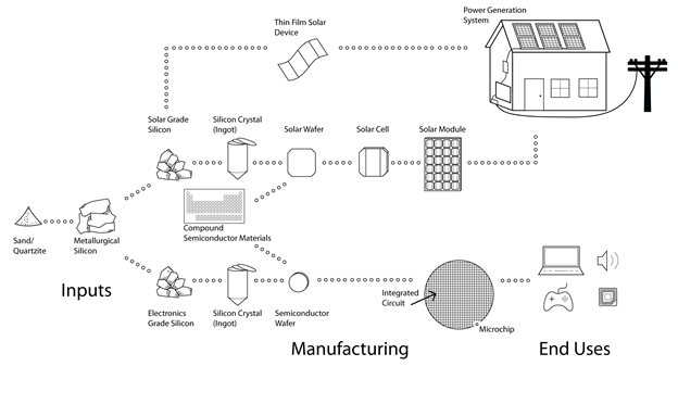
Semiconductor Manufacturing Process
The preferences in this report relate to supplies and materials used in different stages of the semiconductor manufacturing process. The exhibits included in the What is the Preference? tab show the supply chain and manufacturing process for semiconductors from inputs through end uses. The boxes on each exhibit highlight the supplies and materials covered by the relevant preference. In general terms, the semiconductor manufacturing process:
- Begins with a raw material like sand which is smelted and purified into solar or electronic grade silicon.
- The silicon is grown into crystals (also known as ingots) and then sliced into thin solar or semiconductor wafers. Wafers can also be produced from other materials called compound semiconductors, which have similar electronic properties to silicon.
- The silicon wafers are processed to create integrated circuits, which are then cut and packaged into individual microchips. Similarly, the solar wafers are processed to make solar modules.
- Integrated circuits are used to make many types of end products, including computers, video games, audio equipment, radio frequency identification (RFID) tags, and sensors for industrial machinery, medical devices and avionics.
- Solar modules are combined in various forms to generate electricity from sunlight.
Semiconductor Employment in Washington
The Legislature has identified the semiconductor industry as one of the state’s key industry clusters. The Bureau of Labor Statistics (BLS) provides semiconductor employment data by state and by county.
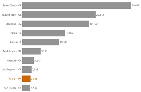
In 2014, Washington ranked 12th in the nation in the number of semiconductor sector employees, but was lower than neighboring states California, Oregon and Idaho. This ranking was based on all businesses in the industry, not just businesses that are eligible for the preferences.
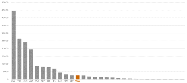
Clark County, with 92% of the state’s semiconductor jobs, ranked 9th in the nation in county semiconductor sector employment.
What are the public policy objectives that provide a justification for the tax preference? Is there any documentation on the purpose or intent of the tax preference?
All of the semiconductor preferences were enacted prior to the Legislature’s requirement to provide a performance statement.
The Legislature expressed its intent for these semiconductor preferences to meet the following objectives:
Induce Significant Construction Projects
The Legislature required semiconductor businesses to make an investment in order for the tax preferences to take effect:
- For the 2003 preferences, the Legislature required an investment of at least $1 billion in a semiconductor microchip fabrication facility;
- For the 2006 preferences, the Legislature required an investment of at least $350 million in a semiconductor materials fabrication facility.
The Legislature noted that these major investments in significant construction projects would create jobs and bring many indirect benefits to the state during the construction phase.
Retain, Expand, and Attract Semiconductor Businesses
The Legislature stated that tax incentives for the semiconductor cluster are important in both retention and expansion of existing businesses and attraction of new ones. The intent statements recognized the semiconductor industry, including the design and manufacture of semiconductor materials, as one of the state’s key industry clusters.
Family-Wage Jobs
The Legislature noted that the welfare of the people of the state is positively impacted through the encouragement and expansion of family wage employment in the state’s manufacturing industries. Presumably these legislative intent statements applied to jobs in semiconductor manufacturing.
What evidence exists to show that the tax preference has contributed to the achievement of any of the public policy objectives?
There are mixed results on inducing significant construction projects. The $1 billion investment necessary for the 2003 preferences never took place, so those preferences have never taken effect and are not meeting their public policy objectives.
For the 2006 preferences, there are mixed results on the other objectives.
Significant Construction Projects
No firm has invested the required $1 billion to build a microchip fabrication facility. Absent this requirement being met, the six 2003 preferences have never gone into effect and are not meeting their public policy objectives.
In contrast, at least one business made the $350 million investment required for the two 2006 preferences to take effect, and at least one significant semiconductor construction project has been completed. The Department of Revenue (DOR) gave notice that the two preferences were in effect as of December 2006. DOR did not identify the business.
The remainder of the evidence section focuses on the two preferences that are in use.
Retain, Expand, and Attract Semiconductor Businesses
Between 2006 and 2014, the net number of businesses in the semiconductor sector increased from 16 to 18. However, the number of semiconductor businesses receiving the reduced B&O rate decreased from three to two. So the net increase in semiconductor businesses did not come from businesses receiving the reduced B&O rate.
In the intent section for the 2006 legislation, the Legislature referenced the semiconductor industry “cluster,” which it described as including the design and manufacturing of semiconductor materials. JLARC staff analyzed Employment Security Department (ESD) data reported by businesses that are classified as part of the Semiconductor and Related Device Manufacturing sector. This classification is broader than the activities covered by the B&O preference.
The net increase in the number of businesses in the overall sector between 2006 and 2014 is a mix of retained and new businesses as well as a reduction from businesses that no longer report to ESD. They may have moved, closed, or merged with other businesses.
In 2014, four businesses reported using the sales and use tax preference. Due to a lack of reporting, there is no comparative figure for 2006.
Family-Wage Jobs
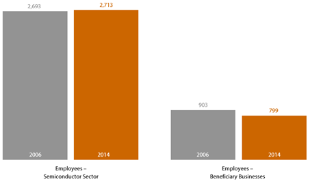
Matching the pattern for the number of businesses, employment in the semiconductor sector as a whole increased slightly (less than one percent) between 2006 and 2014. However, employment in the businesses receiving the reduced B&O rate declined 11.5 percent. So the slight increase in the number of jobs in the semiconductor sector did not come from businesses receiving the reduced B&O rate.
Employment for the semiconductor sector as a whole increased from 2,693 jobs in 2006 to 2,713 jobs in 2014. During the same period, employment in semiconductor businesses receiving the reduced B&O rate declined from 903 to 799, a loss of 104 jobs. Employment numbers for businesses using the sales and use tax preference are not disclosable due to the combination of different forms used to report to DOR. See the Reporting Issues tab for more information.
See the Other Relevant Background tab for how Washington ranks compared to other states.
Job Quality – “Family Wage”
The Legislature did not define what it meant by “family wage employment”. JLARC staff used two measures for comparison:
- The state’s private sector median wage, $21.48 per hour; and
- $60,000 per year, based on prime sponsor testimony.
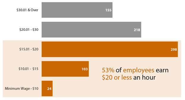
Information on wages and benefits is available for 2014 from the two semiconductor businesses receiving the reduced B&O rate:
- 53 percent of employees earned $20 an hour or less, putting their wages below both the private sector median wage and the wage level identified in testimony;
- Between 88 and 93 percent of employees were eligible for medical benefits, and 88 percent of employees enrolled in medical plans.
Wage and benefit information is not disclosable for the businesses using the sales and use tax preference due to the combination of different forms used to report to DOR. See the Reporting Issues tab for more information.
Note: Job numbers add to 798 rather than 799 due to rounding of numbers reported within the hourly wage bands.
|
Beneficiary
Businesses |
Number of employees |
Percent eligible
for medical benefits |
Percent of
employees enrolled in medical plans |
Average monthly
employer contribution |
Average employee
premium responsibility |
Dependent coverage |
|
S E H America Inc. |
782 |
93% |
88% |
$384 |
10% |
Yes, with additional premium |
|
Galaxy Compound
Semiconductor Inc. |
17 |
88% |
88% |
$135 |
20% |
Yes, with additional premium |
To what extent will continuation of the tax preference contribute to these public policy objectives?
It is unclear to what extent continuation of the preferences will contribute to the public policy objectives:
- The 2003 preferences have yet to induce the required investment to take effect. It is unclear whether the 2006 preferences will induce any additional significant construction projects now that the initial required investment has occurred.
- While there have been slight increases in the number of businesses and jobs in the semiconductor sector as a whole, these increases have not come from businesses receiving the reduced B&O rate.
- For the businesses that are using the preferences, it is unclear whether the amount saved from the preferences relative to income from gross sales is enough to lead to business or job retention or expansion. In 2014, tax savings from the preferences equated to approximately 1/3 of one percent of gross sales for businesses using the sales and use tax exemption.
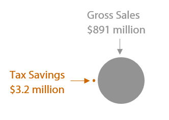
To compare tax savings with gross sales in 2014,
- JLARC staff used the 2014 savings reported by beneficiaries of the sales and use tax preference ($2.3 million) combined with an estimate of 2014 tax savings for the beneficiaries of the B&O preference ($855,000). The actual amount of 2014 B&O savings is not disclosable. JLARC staff based their estimate of B&O savings on information reported by beneficiaries between 2007 and 2009, when this information was disclosable. Estimated total tax savings in 2014 from both the B&O and sales and use preferences is $3.155 million.
- JLARC staff used total gross sales reported for 2014 by the beneficiaries of the sales and use tax preference ($891 million). The gross sales for beneficiaries of the B&O preference are not included because that information is not disclosable.
Who are the entities whose state tax liabilities are directly affected by the tax preference?
There are no beneficiaries for the six preferences passed in 2003 because the required level of private investment to trigger their taking effect has not occurred.
The following information is for beneficiaries of the two tax preferences passed in 2006:
Direct Beneficiaries
In 2014, the beneficiaries of the reduced B&O tax rate were two businesses that manufacture or process semiconductor materials.
In that same year, the beneficiaries of the sales and use tax exemption were four businesses that use gases and chemicals in the production of semiconductor materials.
Indirect Beneficiaries
To the extent that the tax savings are passed on to customers of semiconductor materials or lead to increased purchases from suppliers, other businesses in the semiconductor cluster may be indirect beneficiaries of the preferences.
Three Reporting Issues
Three reporting issues complicate estimates of beneficiary savings and estimates of the number of family wage jobs offered by businesses that use the preferences.
Beneficiary Savings for B&O Preference Not Disclosable
Businesses using the B&O reduced tax rate are required to report their qualifying manufacturing activities on a separate line of their individual tax returns. Tax return data can only be disclosed in the aggregate and if three or more businesses report using the reduced rate. In 2014, less than three businesses reported using the rate so the information is not disclosable.
The Legislature passed SB 5882 in 2013 authorizing disclosure of tax return information after 24 months following the date a return is filed. The reduced B&O rate for semiconductor materials was enacted in 2006. The provisions of SB 5882 authorizing disclosure are not applicable to this preference unless it is modified or extended in the future.
Businesses using the B&O reduced tax rate are also required to file an Annual Report with the Department of Revenue (DOR). The Annual Report includes information on employment and wages but does not require businesses to report their tax savings.
Employment and Wage Estimates for Sales and Use Tax Exemption Not Disclosable
Businesses using the sales and use tax exemption are required to file an Annual Survey with DOR. However, if the same businesses also use the reduced B&O rate, they have the option of filing an Annual Report instead. Several businesses chose to do so in 2014. The result is that fewer than three businesses filed an Annual Survey. Employment and wage information from the Annual Survey is not disclosable if fewer than three businesses report to DOR.
Inconsistent Reporting Requirements Result in Incomplete Information
Beneficiaries of the reduced B&O rate are required to file a different report to DOR than beneficiaries of the sales and use tax exemption. Businesses using both preferences can choose to file only the Annual Report and Buyer Addendum. The reports contain different types of information and neither one provides a complete picture of beneficiary savings and employment and wage data for all businesses using the preferences.
- Businesses using a reduced B&O rate must file an Annual Report with DOR. This includes employment information by occupation, such as number of employees, and percent of employees in different hourly wage categories. It does not include the amount of savings the businesses claimed from the preferential rate.
- Businesses using the sales and use tax exemption must file an Annual Survey with DOR. This includes aggregate employment information for the business, rather than employment by occupation. It also groups employees by annual wages rather than hourly wages. Unlike the Annual Report, the Annual Survey includes the amount of savings businesses claimed from the exemption.
- Businesses using both preferences can choose to file an Annual Report and a Buyer Addendum instead of the Annual Survey. This results in varying employment information collected on businesses using the sales and use tax exemption.
To obtain complete information on employment and tax savings for businesses using both preferences, all businesses would need to submit the same form to DOR, regardless of which preference they are taking. Employment and wage information on the Annual Report forms is publicly disclosable. This information on the Annual Survey is not currently disclosable.
What are the past and future tax revenue and economic impacts of the tax preference to the taxpayer and to the government if it is continued?
JLARC staff estimate the direct beneficiary savings from the sales and use tax exemption for Fiscal Year 2015 is $2.2 million. The estimated beneficiary savings for the sales and use tax exemption for the 2017-19 Biennium is $3.2 million.
Estimated beneficiary savings for the preferential B&O tax rate are not disclosable because fewer than three taxpayers have claimed the preference since 2010. Between 2007 and 2009, when there were at least three taxpayers, the annual beneficiary savings averaged $875,000.
|
Fiscal
Year |
State
Sales Tax |
Local
Sales Tax |
Total
Beneficiary Savings from Sales Tax |
Reduced
B&O Tax Rate |
|
2014 |
$1,800,000 |
$500,000 |
$2,300,000 |
Not Disclosable |
|
2015 |
$1,700,000 |
$500,000 |
$2,200,000 |
Not Disclosable |
|
2016 |
$1,800,000 |
$500,000 |
$2,300,000 |
Not Disclosable |
|
2017 |
$1,800,000 |
$500,000 |
$2,300,000 |
Not Disclosable |
|
2018 |
$1,800,000 |
$500,000 |
$2,300,000* |
Not Disclosable |
|
2019 (7/1/18-12/1/18;
|
$700,000 |
$200,000 |
$900,000 |
Not Disclosable |
|
2017-19 |
$2,500,000 |
$7,000,000 |
$3,200,000 |
Not Disclosable |
Note: This estimate may be overstated because part of the sales and use tax exemption expires in 2017. The expiring part of the exemption relates to semiconductor materials that are used in solar energy systems.
If the tax preference were to be terminated, what would be the negative effects on the taxpayers who currently benefit from the tax preference and the extent to which the resulting higher taxes would have an effect on employment and the economy?
If the tax preferences were terminated, semiconductor businesses that are currently benefiting from the preferences would pay more in B&O, sales, and use taxes. The effect on employment and the economy would depend on the extent to which these manufacturers could absorb this increased cost or pass it along to their customers.
Do other states have a similar tax preference and what potential public policy benefits might be gained by incorporating a corresponding provision in Washington?
Some states, like Washington, provide incentives with statutes specifically targeting semiconductor manufacturers. Other states, like California and Oregon, use different tools and approaches that benefit many industries, including semiconductors.
Idaho exempts semiconductor businesses from paying sales tax on tangible personal property used in, or to maintain, clean rooms. Clean rooms are manufacturing areas with low levels of environmental pollutants such as dust, airborne microbes, aerosol particles and chemical vapors. This exemption is in addition to Idaho’s broader Production Exemption, which applies to chemicals and catalysts used to change a product in the manufacturing process.
Arizona exempts semiconductor clean rooms from sales and use tax. This exemption is in addition to the broader sales and use tax exemption for chemicals used in manufacturing and processing. Clean rooms are also assessed as tangible personal property for the purpose of property taxes, which allows for preferable tax treatment.
Florida exempts semiconductor, defense, and space technology businesses from sales and use tax on their machinery and equipment.
The District of Columbia offers all qualified high-tech companies, including semiconductor businesses, a package of tax incentives including a reduction or exemption from income tax and property tax, plus tax credits for relocation and hiring certain types of employees.
California has the highest number of semiconductor employees in the country. It offers the California Competes Tax Credit which is a negotiable credit available to businesses locating or growing in California. The state also offers a sales and use tax exclusion for advanced manufacturing, which includes semiconductors. Other California incentive programs include cash reimbursement for employee training costs, industrial development bonds and small business loan guarantees.
Oregon’s incentive program was mentioned in public testimony during hearings for the Washington preferences. Oregon currently has three strategic investment agreements with two semiconductor businesses, providing partial property tax exemptions.
Preferences in effect
Intent Statement
Findings—Intent—2006 c 84: "The legislature finds that the welfare of the people of the state of Washington is positively impacted through the encouragement and expansion of family wage employment in the state's manufacturing industries. The legislature further finds that targeting tax incentives to focus on key industry clusters is an important business climate strategy. Washington state has recognized the semiconductor industry, which includes the design and manufacture of semiconductor materials, as one of the state's existing key industry clusters. Businesses in this cluster in the state of Washington are facing increasing pressure to expand elsewhere. The sales and use tax exemptions for manufacturing machinery and equipment enacted by the 1995 legislature improved Washington's ability to compete with other states for manufacturing investment. In 2003 the legislature enacted comprehensive tax incentives for the semiconductor cluster that address activities of the lead product industry and its suppliers and customers. These tax incentives are contingent on the investment of at least one billion dollars in a new semiconductor microchip fabrication facility in this state, which has not occurred. This investment criteria failed to recognize the significance of potential investment in the advanced semiconductor materials sector. Therefore, the legislature intends to complement existing comprehensive tax incentives for the semiconductor cluster to address activities of the advanced semiconductor materials product industry and its suppliers and customers. Tax incentives for the semiconductor cluster are important in both retention and expansion of existing businesses and attraction of new businesses, all of which will strengthen this cluster. The legislature also recognizes that the semiconductor industry involves major investment that results in significant construction projects, which will create jobs and bring many indirect benefits to the state during the construction phase." [ 2006 c 84 § 1.]
Preferences not in effect
Intent Statement
Findings—Intent—2003 c 149: "The legislature finds that the welfare of the people of the state of Washington is positively impacted through the encouragement and expansion of family wage employment in the state's manufacturing industries. The legislature further finds that targeting tax incentives to focus on key industry clusters is an important business climate strategy. The Washington competitiveness council has recognized the semiconductor industry, which includes the design and manufacture of semiconductor materials, as one of the state's existing key industry clusters. Businesses in this cluster in the state of Washington are facing increasing pressure to expand elsewhere. The sales and use tax exemptions for manufacturing machinery and equipment enacted by the 1995 legislature improved Washington's ability to compete with other states for manufacturing investment. However, additional incentives for the semiconductor cluster need to be put in place in recognition of the unique forces and global issues involved in business decisions that key businesses in this cluster face.
Therefore, the legislature intends to enact comprehensive tax incentives for the semiconductor cluster that address activities of the lead product industry and its suppliers and customers. Tax incentives for the semiconductor cluster are important in both retention and expansion of existing business and attraction of new businesses, all of which will strengthen this cluster. The legislature also recognizes that the semiconductor industry involves major investment that results in significant construction projects, which will create jobs and bring many indirect benefits to the state during the construction phase." [ 2003 c 149 § 1.]
Preferences in effect
RCW 82.04.2404
Manufacturers—Processors for hire—Semiconductor materials. (Expires December 1, 2018.)
(1) Upon every person engaging within this state in the business of manufacturing or processing for hire semiconductor materials, as to such persons the amount of tax with respect to such business is, in the case of manufacturers, equal to the value of the product manufactured, or, in the case of processors for hire, equal to the gross income of the business, multiplied by the rate of 0.275 percent.
(2) For the purposes of this section "semiconductor materials" means silicon crystals, silicon ingots, raw polished semiconductor wafers, and compound semiconductor wafers.
(3) A person reporting under the tax rate provided in this section must file a complete Annual Report with the department under RCW 82.32.534.
(4) This section expires December 1, 2018.
[ 2010 c 114 § 105; 2006 c 84 § 2.]
RCW 82.08.9651
Exemptions—Gases and chemicals used in production of semiconductor materials. (Expires December 1, 2018.)
(1) The tax levied by RCW 82.08.020 does not apply to sales of gases and chemicals used by a manufacturer or processor for hire in the production of semiconductor materials. This exemption is limited to gases and chemicals used in the production process to grow the product, deposit or grow permanent or sacrificial layers on the product, to etch or remove material from the product, to anneal the product, to immerse the product, to clean the product, and other such uses whereby the gases and chemicals come into direct contact with the product during the production process, or uses of gases and chemicals to clean the chambers and other like equipment in which such processing takes place. For the purposes of this section, "semiconductor materials" has the meaning provided in RCW 82.04.2404 and 82.04.294(3).
(2)(a) Except as provided under (b) of this subsection (2), a person claiming the exemption under this section must file a complete Annual Survey with the department under RCW 82.32.585.
(b) A person claiming the exemption under this section and who is required to file a complete Annual Report with the department under RCW 82.32.534 as a result of claiming the tax preference provided by RCW 82.04.2404 is not also required to file a complete Annual Survey under RCW 82.32.585.
(3) No application is necessary for the tax exemption. The person is subject to all of the requirements of chapter 82.32 RCW.
(4) This section expires December 1, 2018.
[ 2014 c 97 § 405; 2010 c 114 § 124; 2009 c 469 § 502; 2006 c 84 § 3.]
RCW 82.12.9651
Exemptions—Gases and chemicals used in production of semiconductor materials. (Expires December 1, 2018.)
(1) The provisions of this chapter do not apply with respect to the use of gases and chemicals used by a manufacturer or processor for hire in the production of semiconductor materials. This exemption is limited to gases and chemicals used in the production process to grow the product, deposit or grow permanent or sacrificial layers on the product, to etch or remove material from the product, to anneal the product, to immerse the product, to clean the product, and other such uses whereby the gases and chemicals come into direct contact with the product during the production process, or uses of gases and chemicals to clean the chambers and other like equipment in which such processing takes place. For purposes of this section, "semiconductor materials" has the meaning provided in RCW 82.04.2404 and 82.04.294(3).
(2)(a) Except as provided under (b) of this subsection (2), a person claiming the exemption under this section must file a complete Annual Survey with the department under RCW 82.32.585.
(b) A person claiming the exemption under this section and who is required to file a complete Annual Report with the department under RCW 82.32.534 as a result of claiming the tax preference provided by RCW 82.04.2404 is not also required to file a complete Annual Survey under RCW 82.32.585.
(3) No application is necessary for the tax exemption. The person is subject to all of the requirements of chapter 82.32 RCW.
(4) This section expires December 1, 2018.
[ 2014 c 97 § 406; 2010 c 114 § 130; 2009 c 469 § 503; 2006 c 84 § 4.]
RCW 82.04.294
Tax on manufacturers or wholesalers of solar energy systems. (Expires June 30, 2017.)
(1) Upon every person engaging within this state in the business of manufacturing solar energy systems using photovoltaic modules or stirling converters, or of manufacturing solar grade silicon, silicon solar wafers, silicon solar cells, thin film solar devices, or compound semiconductor solar wafers to be used exclusively in components of such systems; as to such persons the amount of tax with respect to such business is, in the case of manufacturers, equal to the value of the product manufactured, or in the case of processors for hire, equal to the gross income of the business, multiplied by the rate of 0.275 percent.
(2) Upon every person engaging within this state in the business of making sales at wholesale of solar energy systems using photovoltaic modules or stirling converters, or of solar grade silicon, silicon solar wafers, silicon solar cells, thin film solar devices, or compound semiconductor solar wafers to be used exclusively in components of such systems, manufactured by that person; as to such persons the amount of tax with respect to such business is equal to the gross proceeds of sales of the solar energy systems using photovoltaic modules or stirling converters, or of the solar grade silicon to be used exclusively in components of such systems, multiplied by the rate of 0.275 percent.
(3) Silicon solar wafers, silicon solar cells, thin film solar devices, solar grade silicon, or compound semiconductor solar wafers are "semiconductor materials" for the purposes of RCW 82.08.9651 and 82.12.9651.
(4) The definitions in this subsection apply throughout this section.
(a) "Compound semiconductor solar wafers" means a semiconductor solar wafer composed of elements from two or more different groups of the periodic table.
(b) "Module" means the smallest nondivisible self-contained physical structure housing interconnected photovoltaic cells and providing a single direct current electrical output.
(c) "Photovoltaic cell" means a device that converts light directly into electricity without moving parts.
(d) "Silicon solar cells" means a photovoltaic cell manufactured from a silicon solar wafer.
(e) "Silicon solar wafers" means a silicon wafer manufactured for solar conversion purposes.
(f) "Solar energy system" means any device or combination of devices or elements that rely upon direct sunlight as an energy source for use in the generation of electricity.
(g) "Solar grade silicon" means high-purity silicon used exclusively in components of solar energy systems using photovoltaic modules to capture direct sunlight. "Solar grade silicon" does not include silicon used in semiconductors.
(h) "Stirling converter" means a device that produces electricity by converting heat from a solar source utilizing a stirling engine.
(i) "Thin film solar devices" means a nonparticipating substrate on which various semiconducting materials are deposited to produce a photovoltaic cell that is used to generate electricity.
(5) A person reporting under the tax rate provided in this section must file a complete Annual Survey with the department under RCW 82.32.585.
(6) This section expires June 30, 2017.
Preferences not in effect
RCW 82.04.240
Tax on manufacturers. (Contingent effective date; contingent expiration of subsection.)
(1) Upon every person engaging within this state in business as a manufacturer, except persons taxable as manufacturers under other provisions of this chapter; as to such persons the amount of the tax with respect to such business is equal to the value of the products, including byproducts, manufactured, multiplied by the rate of 0.484 percent.
(2)(a) Upon every person engaging within this state in the business of manufacturing semiconductor materials, as to such persons the amount of tax with respect to such business is, in the case of manufacturers, equal to the value of the product manufactured, or, in the case of processors for hire, equal to the gross income of the business, multiplied by the rate of 0.275 percent. For the purposes of this subsection "semiconductor materials" means silicon crystals, silicon ingots, raw polished semiconductor wafers, compound semiconductors, integrated circuits, and microchips.
(b) A person reporting under the tax rate provided in this subsection (2) must file a complete annual report with the department under RCW 82.32.534.
(c) This subsection (2) expires twelve years after *the effective date of this act.
(3) The measure of the tax is the value of the products, including byproducts, so manufactured regardless of the place of sale or the fact that deliveries may be made to points outside the state.
[ 2010 c 114 § 104; 2003 c 149 § 3; 1998 c 312 § 3; 1993 sp.s. c 25 § 102; 1981 c 172 § 1; 1979 ex.s. c 196 § 1; 1971 ex.s. c 281 § 3; 1969 ex.s. c 262 § 34; 1967 ex.s. c 149 § 8; 1965 ex.s. c 173 § 5; 1961 c 15 § 82.04.240. Prior: 1959 c 211 § 1; 1955 c 389 § 44; prior: 1950 ex.s. c 5 § 1, part; 1949 c 228 § 1, part; 1943 c 156 § 1, part; 1941 c 178 § 1, part; 1939 c 225 § 1, part; 1937 c 227 § 1, part; 1935 c 180 § 4, part; Rem. Supp. 1949 § 8370-4, part.]
RCW 82.04.426
Exemptions—Semiconductor microchips. (Contingent effective date; contingent expiration date.)
(1) The tax imposed by RCW 82.04.240(2) does not apply to any person in respect to the manufacturing of semiconductor microchips.
(2) For the purposes of this section:
(a) "Manufacturing semiconductor microchips" means taking raw polished semiconductor wafers and embedding integrated circuits on the wafers using processes such as masking, etching, and diffusion; and
(b) "Integrated circuit" means a set of microminiaturized, electronic circuits.
(3) A person reporting under the tax rate provided in this section must file a complete annual report with the department under RCW 82.32.534.
(4) This section expires nine years after *the effective date of this act.
[ 2010 c 114 § 110; 2003 c 149 § 2.]
RCW 82.04.448
Credit—Manufacturing semiconductor materials. (Contingent effective date; contingent expiration date.)
(1) Subject to the limits and provisions of this section, a credit is authorized against the tax otherwise due under RCW 82.04.240(2) for persons engaged in the business of manufacturing semiconductor materials. For the purposes of this section "semiconductor materials" has the same meaning as provided in RCW 82.04.240(2).
(2)(a) The credit under this section equals three thousand dollars for each employment position used in manufacturing production that takes place in a new building exempt from sales and use tax under RCW 82.08.965 and 82.12.965. A credit is earned for the calendar year a person fills a position. Additionally a credit is earned for each year the position is maintained over the subsequent consecutive years, up to eight years. Those positions that are not filled for the entire year are eligible for fifty percent of the credit if filled less than six months, and the entire credit if filled more than six months.
(b) To qualify for the credit, the manufacturing activity of the person must be conducted at a new building that qualifies for the exemption from sales and use tax under RCW 82.08.965 and 82.12.965.
(c) In those situations where a production building in existence on *the effective date of this section will be phased out of operation, during which time employment at the new building at the same site is increased, the person is eligible for credit for employment at the existing building and new building, with the limitation that the combined eligible employment not exceed full employment at the new building. "Full employment" has the same meaning as in RCW 82.08.965. The credit may not be earned until the commencement of commercial production, as that term is used in RCW 82.08.965.
(3) No application is necessary for the tax credit. The person is subject to all of the requirements of chapter 82.32 RCW. In no case may a credit earned during one calendar year be carried over to be credited against taxes incurred in a subsequent calendar year. No refunds may be granted for credits under this section.
(4) If at any time the department finds that a person is not eligible for tax credit under this section, the amount of taxes for which a credit has been claimed is immediately due. The department must assess interest, but not penalties, on the taxes for which the person is not eligible. The interest must be assessed at the rate provided for delinquent excise taxes under chapter 82.32 RCW, is retroactive to the date the tax credit was taken, and accrues until the taxes for which a credit has been used are repaid.
(5) A person claiming the credit under this section must file a complete annual report with the department under RCW 82.32.534.
(6) Credits may be claimed after twelve years after *the effective date of this act, for those buildings at which commercial production began before twelve years after *the effective date of this act, subject to all of the eligibility criteria and limitations of this section.
(7) This section expires twelve years after *the effective date of this act.
[ 2010 c 114 § 117; 2003 c 149 § 9.]
RCW 82.08.970
Exemptions—Gases and chemicals used to manufacture semiconductor materials. (Contingent effective date; contingent expiration date.)
(1) The tax levied by RCW 82.08.020 does not apply to sales of gases and chemicals used by a manufacturer or processor for hire in the manufacturing of semiconductor materials. This exemption is limited to gases and chemicals used in the manufacturing process to grow the product, deposit or grow permanent or sacrificial layers on the product, to etch or remove material from the product, to anneal the product, to immerse the product, to clean the product, and other such uses whereby the gases and chemicals come into direct contact with the product during the manufacturing process, or uses of gases and chemicals to clean the chambers and other like equipment in which such processing takes place. For the purposes of this section, "semiconductor materials" has the same meaning as provided in RCW 82.04.240(2).
(2) A person claiming the exemption under this section must file a complete annual report with the department under RCW 82.32.534. No application is necessary for the tax exemption. The person is subject to all of the requirements of chapter 82.32 RCW.
(3) This section expires twelve years after *the effective date of this act.
[ 2010 c 114 § 125; 2003 c 149 § 7.]
RCW 82.12.970
Exemptions—Gases and chemicals used to manufacture semiconductor materials. (Contingent effective date; contingent expiration date.)
(1) The provisions of this chapter do not apply with respect to the use of gases and chemicals used by a manufacturer or processor for hire in the manufacturing of semiconductor materials. This exemption is limited to gases and chemicals used in the manufacturing process to grow the product, deposit or grow permanent or sacrificial layers on the product, to etch or remove material from the product, to anneal the product, to immerse the product, to clean the product, and other such uses whereby the gases and chemicals come into direct contact with the product during the manufacturing process, or uses of gases and chemicals to clean the chambers and other like equipment in which such processing takes place. For purposes of this section, "semiconductor materials" has the same meaning as provided in RCW 82.04.240(2).
(2) A person claiming the exemption under this section must file a complete annual report with the department under RCW 82.32.534. No application is necessary for the tax exemption. The person is subject to all of the requirements of chapter 82.32 RCW.
(3) This section expires twelve years after *the effective date of this act.
[ 2010 c 114 § 131; 2003 c 149 § 8.]
RCW 82.08.965
Exemptions—Semiconductor materials manufacturing. (Contingent effective date; contingent expiration date.)
(1) The tax levied by RCW 82.08.020 does not apply to charges made for labor and services rendered in respect to the constructing of new buildings used for the manufacturing of semiconductor materials, to sales of tangible personal property that will be incorporated as an ingredient or component of such buildings during the course of the constructing, or to labor and services rendered in respect to installing, during the course of constructing, building fixtures not otherwise eligible for the exemption under RCW 82.08.02565(2)(b). The exemption is available only when the buyer provides the seller with an exemption certificate in a form and manner prescribed by the department. The seller must retain a copy of the certificate for the seller's files.
(2) To be eligible under this section the manufacturer or processor for hire must meet the following requirements for an eight-year period, such period beginning the day the new building commences commercial production, or a portion of tax otherwise due will be immediately due and payable pursuant to subsection (3) of this section:
(a) The manufacturer or processor for hire must maintain at least seventy-five percent of full employment at the new building for which the exemption under this section is claimed.
(b) Before commencing commercial production at a new facility the manufacturer or processor for hire must meet with the department to review projected employment levels in the new buildings. The department, using information provided by the taxpayer, must make a determination of the number of positions that would be filled at full employment. This number must be used throughout the eight-year period to determine whether any tax is to be repaid. This information is not subject to the confidentiality provisions of RCW 82.32.330 and may be disclosed to the public upon request.
(c) In those situations where a production building in existence on *the effective date of this section will be phased out of operation during which time employment at the new building at the same site is increased, the manufacturer or processor for hire must maintain seventy-five percent of full employment at the manufacturing site overall.
(d) No application is necessary for the tax exemption. The person is subject to all the requirements of chapter 82.32 RCW. A person claiming the exemption under this section must file a complete annual report with the department under RCW 82.32.534.
(3) If the employment requirement is not met for any one calendar year, one-eighth of the exempt sales and use taxes will be due and payable by April 1st of the following year. The department must assess interest to the date the tax was imposed, but not penalties, on the taxes for which the person is not eligible.
(4) The exemption applies to new buildings, or parts of buildings, that are used exclusively in the manufacturing of semiconductor materials, including the storage of raw materials and finished product.
(5) For the purposes of this section:
(a) "Commencement of commercial production" is deemed to have occurred when the equipment and process qualifications in the new building are completed and production for sale has begun; and
(b) "Full employment" is the number of positions required for full capacity production at the new building, for positions such as line workers, engineers, and technicians.
(c) "Semiconductor materials" has the same meaning as provided in RCW 82.04.240(2).
(6) No exemption may be taken after twelve years after *the effective date of this act, however all of the eligibility criteria and limitations are applicable to any exemptions claimed before that date.
(7) This section expires twelve years after *the effective date of this act.
[ 2010 c 114 § 123; 2003 c 149 § 5.]
RCW 82.12.965
Exemptions—Semiconductor materials manufacturing. (Contingent effective date; contingent expiration date.)
(1) The provisions of this chapter do not apply with respect to the use of tangible personal property that will be incorporated as an ingredient or component of new buildings used for the manufacturing of semiconductor materials during the course of constructing such buildings or to labor and services rendered in respect to installing, during the course of constructing, building fixtures not otherwise eligible for the exemption under RCW 82.08.02565(2)(b).
(2) The eligibility requirements, conditions, and definitions in RCW 82.08.965 apply to this section, including the filing of a complete annual report with the department under RCW 82.32.534.
(3) No exemption may be taken twelve years after *the effective date of this act, however all of the eligibility criteria and limitations are applicable to any exemptions claimed before that date.
(4) This section expires twelve years after *the effective date of this act.
[ 2010 c 114 § 129; 2003 c 149 § 6.]
RCW 84.36.645
Semiconductor materials. (Contingent effective date; contingent expiration date.)
(1) Machinery and equipment exempt under RCW 82.08.02565 or 82.12.02565 used in manufacturing semiconductor materials at a building exempt from sales and use tax and in compliance with the employment requirement under RCW 82.08.965 and 82.12.965 are exempt from property taxation. "Semiconductor materials" has the same meaning as provided in RCW 82.04.240(2).
(2) A person seeking this exemption must make application to the county assessor, on forms prescribed by the department.
(3) A person claiming an exemption under this section must file a complete annual report with the department under RCW 82.32.534.
(4) This section is effective for taxes levied for collection one year after *the effective date of this act and thereafter.
(5) This section expires December 31st of the year occurring twelve years after *the effective date of this act, for taxes levied for collection in the following year.
[ 2010 c 114 § 150; 2003 c 149 § 10.]
RCW 82.32.790
Tax incentives contingent upon semiconductor microchip fabrication facility siting and operation.
(1)(a) Section 206, chapter 106, Laws of 2010, sections 104, 110, 117, 123, 125, 129, 131, and 150, chapter 114, Laws of 2010, section 3, chapter 461, Laws of 2009, section 7, chapter 300, Laws of 2006, and section 4, chapter 149, Laws of 2003 are contingent upon the siting and commercial operation of a significant semiconductor microchip fabrication facility in the state of Washington.
(b) For the purposes of this section:
(i) "Commercial operation" means the same as "commencement of commercial production" as used in RCW 82.08.965.
(ii) "Semiconductor microchip fabrication" means "manufacturing semiconductor microchips" as defined in RCW 82.04.426.
(iii) "Significant" means the combined investment of new buildings and new machinery and equipment in the buildings, at the commencement of commercial production, will be at least one billion dollars.
(2) Chapter 149, Laws of 2003 takes effect the first day of the month in which a contract for the construction of a significant semiconductor fabrication facility is signed, as determined by the director of the department of revenue.
(3)(a) The department of revenue must provide notice of the effective date of sections 104, 110, 117, 123, 125, 129, 131, and 150, chapter 114, Laws of 2010[,] section 3, chapter 461, Laws of 2009, section 7, chapter 300, Laws of 2006, and section 4, chapter 149, Laws of 2003 to affected taxpayers, the legislature, and others as deemed appropriate by the department.
(b) If, after making a determination that a contract has been signed and chapter 149, Laws of 2003 is effective, the department discovers that commencement of commercial production did not take place within three years of the date the contract was signed, the department must make a determination that chapter 149, Laws of 2003 is no longer effective, and all taxes that would have been otherwise due are deemed deferred taxes and are immediately assessed and payable from any person reporting tax under RCW 82.04.240(2) or claiming an exemption or credit under section 2 or 5 through 10, chapter 149, Laws of 2003. The department is not authorized to make a second determination regarding the effective date of chapter 149, Laws of 2003.
[ 2010 c 114 § 201; 2010 c 106 § 401; 2009 c 461 § 9; 2006 c 300 § 12; 2003 c 149 § 12.]
- Legislative Auditor Recommendation
- Letter from Commission Chair
- Commissioners' Recommendation
- Agency Response
Legislative Auditor Recommendation
- For the six preferences not currently in effect, the Legislature should terminate the preferences because they have not been used in the thirteen years since they were enacted.
- No firm has made the required investment of at least $1 billion in a new microchip fabrication facility located in Washington. The tax preferences are contingent on this investment.
- The legislative history of the six preferences indicates that the Legislature wanted to provide incentive for a specific firm, Wafertech, to stay in Washington. Wafertech still remains in the state.
Legislation Required: Yes.
Fiscal Impact: None.
- The Legislature should review and clarify the two preferences currently in effect because while there has been one significant construction project, it is unclear what employment outcomes the Legislature wants to achieve. As part of the clarification, the Legislature should add uniform reporting requirements and targets for employment growth and wages to facilitate future reviews.
- It is unclear whether the preferences will induce any additional significant construction projects now that the initial required investment has occurred.
- While there have been slight increases in the net number of businesses and in jobs in the semiconductor sector as a whole, these increases have not come from businesses receiving the reduced B&O rate. The number of businesses receiving the reduced B&O rate has declined from three to two, and their employment has decreased by 11.5 percent since 2006.
- To facilitate future reviews of the preferences, the Legislature should consider setting targets for employment growth and wages. Additionally, the Legislature should consider requiring uniform reporting requirements for all businesses that claim one or both preferences and authorizing disclosure of tax savings by those businesses. This would provide a more complete picture of beneficiary savings and allow for meaningful comparisons of employment and wages among the businesses using the preferences.
Both the reduced B&O rate and the sales and use tax exemption expire on December 1, 2018. The part of the sales and use tax exemption relating to solar energy systems expires on June 30, 2017.
Legislation Required: Yes.
Fiscal Impact: Depends on legislative action.


The Commission endorses the Legislative Auditor’s recommendation.
In addition to JLARC staff’s research, a recent research paper released by the Congressional Research Service (CRS) on the U.S. semiconductor industry highlights some important points. First, the CRS study finds that about 87% of fabrication is located outside of the U.S. with little evidence this will change significantly in the future. Second, between 2001 and 2015 U.S. employment in semiconductor manufacturing has fallen 38%. Third, the decline in employment reflects both the shift of production to outside of the U.S.; increasing automation of production facilities; and a shift in favor of U.S. employment focused on semiconductor design work. The trends laid out by the CRS paper suggest that the current set of preferences will be, for the foreseeable future, underutilized or not utilized.
Joint Department of Revenue and Office of Financial Management Response